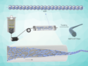
Trigonal selenium (t-Se) has interesting and potentially useful properties. It is a semiconductor material with high photoconductivity, piezoelectricity, and thermoelectricity, for example. Nanostructures of the material could be particularly useful for a range of applications. However, due to the chain structure of t-Se (pictured), it usually forms one-dimensional nanostructures, such as nanowires and nanobelts. These structures can have poor electrical transport properties, which could be improved by using 2D nanostructures instead.
Peide D. Ye, Purdue University, West Lafayette, IN, USA, and colleagues have synthesized high-quality 2D selenium nanosheets in comparatively large sizes. The team used a physical vapor deposition (PVD) method with Se powder (heated to 210 °C) as a precursor and a Si substrate (heated to 100 °C) to grow the nanosheets on. The resulting nanosheets were characterized using scanning transmission electron microscopy (STEM) and angle-resolved Raman spectroscopy. The nanosheets reached average edge lengths of 30 μm with a thickness of down to 5 nm.
Due to the chain-like structure of selenium in the nanosheets, the synthesized material has anisotropic properties within the plane. The team used the material in field-effect transistors (FETs) and found good conduction properties. When used in phototransistors, the nanosheets also demonstrated a high photoresponsivity. According to the researchers, the material could have potential for electronic and optoelectronic applications.
- Controlled Growth of a Large-Size 2D Selenium Nanosheet and Its Electronic and Optoelectronic Applications,
Jingkai Qin, Gang Qiu, Jie Jian, Hong Zhou, Lingming Yang, Adam Charnas, Dmitry Y. Zemlyanov, Cheng-Yan Xu, Xianfan Xu, Wenzhuo Wu, Haiyan Wang, Peide D. Ye,
ACS Nano 2017.
DOI: 10.1021/acsnano.7b04786