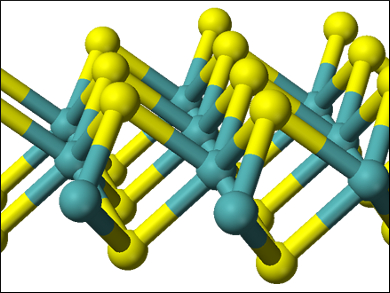
Transition metal dichalcogenides with 2D structures, such as molybdenum disulfide (MoS2), can be useful for electronic and optoelectronic technologies. One important property that determines the materials’ performance in transistors or photodetectors is carrier mobility. This mobility is dependent on scattering time, i.e., how long the carrier is accelerated by the electric field until it collides with something that changes its direction and/or energy.
Gerasimos Konstantatos, Barcelona Institute of Science and Technology and Institució Catalana de Recerca i Estudis Avançats (ICREA), Barcelona, Spain, and colleagues have created a simple technique to suppress both Coulomb scattering and electron–phonon scattering in MoS2-based devices using an overlayer composed of HfO2. The researchers grew 2D layers of MoS2 using chemical vapor deposition (CVD). A thin overlayer of HfO2 was then deposited on the MoS2 using atomic layer deposition (ALD). Metal electrodes for the devices were created using laser writing lithography.
The approach allowed the researchers to create an MoS2 transistor with a charge carrier mobility of 60 cm2 V–1 s–1, an improvement over pristine MoS2. When the MoS2 layer is covered with HfO2, the scattering is naturally suppressed due to the removal of surface adsorbates and the presence of a high dielectric screening. Additionally, homopolar phonons are quenched, which leads to the suppression of electron–phonon scattering.
- High carrier mobility in monolayer CVD-grown MoS2 through phonon suppression,
Nengjie Huo, Yujue Yang, Yu-Ning Wu, Xiao-Guang Zhang, Sokrates T. Pantelides, Gerasimos Konstantatos,
Nanoscale 2018.
https://doi.org/10.1039/c8nr04416c