In 1931, Ernst Ruska invented the transmission electron microscope (TEM). Instead of refraction of light beams as in a light microscope, electron beams are deflected. The much smaller wavelength of the electron beams allows a magnification that is thousands of times higher. As electrons are charged particles, electromagnetic fields have been used as lenses. Researchers have continually pursued better spatial resolution.
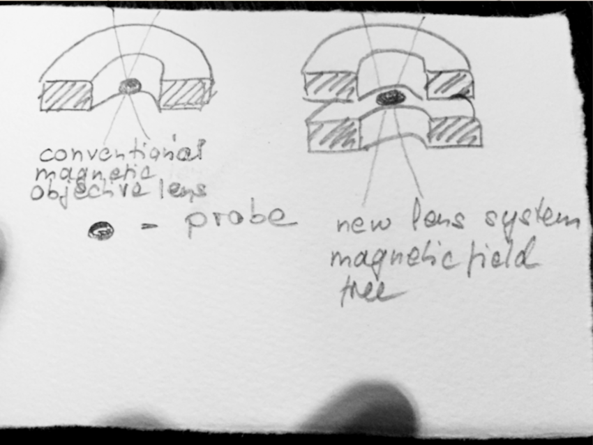
One critical disadvantage of current magnetic condenser-objective-lens systems for atomic-resolution TEMs/STEMs is that the samples must be inserted into very high magnetic fields of up to 2–3 T. Therefore, atomic-resolution imaging of many important soft/hard magnetic materials, such as silicon steel, have been impossible because the strong field alters or even destroys the material’s magnetic and sometimes physical structure.
Naoya Shibata, University of Tokyo, Japan, and Nanostructures Research Laboratory, Japan Fine Ceramic Center, Atsuta, Nagoya, and colleagues have developed a magnetic objective lens system that realizes a magnetic field free environment at the sample position. The new system contains of two round lenses positioned in an exact mirror-symmetric configuration with respect to the sample plane. This lens system provides extremely small residual magnetic fields at the sample position while placing the strongly excited front/back objective lenses close enough to the sample to obtain the short focus length condition indispensable for atomic-resolution imaging. The team combined this lens system with a higher-order aberration corrector and achieved direct, atom-resolved imaging with sub-Å spatial resolution with a residual magnetic field of less than 0.2 mT at the sample position.
This system should allow atomic structure characterization of any magnetic material, which has hitherto been extremely challenging in TEMs/STEMs. Since this objective lens can also be applied to other existing TEM/STEM imaging and analytical techniques, the researchers think that their achievement should have considerable far-reaching effects across the entire field of transmission electron microscopy.
The grain-oriented silicon-steel sheet is one of the most important soft magnetic engineering materials. This sheet is used as a core material for electric transformers and motors, and its atomic-resolution characterization of individual defects has long been sought. Using the newly developed lens system, the resolved atomic structure of the silicon steel was clearly observed.
- Atomic resolution electron microscopy in a magnetic field free environment,
N. Shibata, Y. Kohno, A. Nakamura, S. Morishita, T. Seki, A. Kumamoto, H. Sawada, T. Matsumoto, S. D. Findlay, Y. Ikuhara,
Nature Communic. 2019.
http://dx.doi.org/10.1038/s41467-019-10281-2