Two-dimensional semiconductors, such as monolayers of MoS2 and MoSe2, have interesting electronic and optical properties. However, they have relatively small band gaps (< 2 eV), which hinder optoelectronic applications involving short wavelengths, i.e., blue and UV light.
Haibo Zeng, Nanjing University of Science and Technology, China, and colleagues have calculated structures and properties of two promising high-band gap 2D semiconductor candidates: arsenene and antimonene (As and Sb monolayers, respectively). The 2D crystals have band gaps of 2.49 eV in the case of As and 2.28 eV for Sb. Attraction between monolayers is predicted to be small enough to allow the synthesis of the 2D species analogous to the facile production of graphene, and the calculated electron mobility is comparatively high.
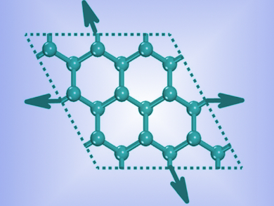
While these properties are promising, both arsenene and antimonene exhibit indirect band gaps, limiting their efficiency for light emission. As it turns out, applying a biaxial tensile strain (pictured) to the monolayer leads to a indirect-to-direct band-gap transition in both species. This could improve the efficiency in optoelectronic applications and also allow their use as mechanical sensors.
- Atomically Thin Arsenene and Antimonene: Semimetal–Semiconductor and Indirect–Direct Band-Gap Transitions,
Shengli Zhang, Zhong Yan, Yafei Li, Zhongfang Chen, Haibo Zeng,
Angew. Chem. Int. Ed. 2015.
DOI: 10.1002/anie.201411246