Atomic Manipulation
Could electron beam manipulation be the answer to constructing nanostructures atom-by-atom? According to work by Ondrej Dyck, Oak Ridge National Laboratory, TN, USA, and colleagues, the answer is yes. The team moved silicon atoms in a graphene lattice using a focused electron beam in a scanning transmission electron microscope (STEM).
It was physicist Richard Feynman who famously laid down a challenge for scientists to build the nano realm from the bottom up almost sixty years ago. At the time, there were no tools that could operate on even small clusters of individual molecules—let alone atoms. The invention of the scanning tunneling microscope (STM) provided the means to work towards finding a way to address Feynman’s challenge. Indeed, in recent years, STM has been responsible for a lot of progress in nanotechnology. Headlines in the popular science press have heralded nanoscopic institutional logos, stick figures, etc.
Alternative Methods
STM, however, has significant limitations, according to Dyck and colleagues. In order to be useful, it requires complex surface science approaches to establish and maintain atomically clean surfaces. Moreover, the products of STM manipulation then further require a complex technological cycle so that the single-atom devices can be integrated with classical semiconductor technologies. “The development process remained slow and required large capital investments to even begin the development,” the team writes. “Thus, alternative methods for atom-by-atom fabrication are of interest.”
“The advancements in STM have been significant and impressive,” Dyck told ChemViews Magazine. “The technique is certainly not inferior, but it offers significant challenges, which leaves the door open for alternative manipulation techniques.”
Manipulative Electron Beams
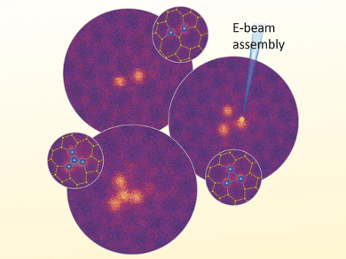
The team used an atomically focused electron beam to introduce silicon substitutional defects and defect clusters into graphene. To prevent the electron beam from inducing irreparable damage to the graphene, a challenge they had faced previously, the team used a strategy where the electron beam was kept in continuous motion. This strategy also has the advantage of producing a real-time updating image to monitor the sample state while the silicon atoms are put into the graphene.
This technique gives the researchers spatial control to within a few nanometers. In a second step, lowering the energy of the beam allows them atomic-level control of the motion of the silicon atoms. They can manipulate the silicon defects in the graphene sheet to bring two or three together to form dimers and trimers (pictured), or form even more complex structures, such as pyramidal tetramers.
Wide Repertoire
“It’s a two-step process,” Dyck explains. “Insertion of the dopants into the lattice and then, movement of the dopants through the lattice to assemble structures.” He adds that the first step is performed with a higher energy beam (100 keV) and the second step is performed with a lower energy (60 keV). “This protocol is highly unusual because switching energy typically takes several hours at a minimum,” Dyck adds. “Here, we highlight the different capabilities accessible to the different energy beams in a single experiment.”
The researchers also point out that other elements can be used to dope graphene, including boron, nitrogen, oxygen, phosphorus, and even metals such as iron, gold, chromium, titanium, palladium, nickel, and aluminum. This dopant repertoire might lend itself to the atom-by-atom construction of quite sophisticated structures within the 2D framework of a graphene sheet. Given the advances being made with respect to the integration of graphene into classical microelectronics technologies, this approach might lead the way to hybrid devices.
Early Stages
The team has captured an image time-series of an atomic-scale electron-beam-assisted chemical reaction occurring with atomic resolution. They also confirmed the nature of their manipulations with density functional theory (DFT) calculations.
The approach is still in its nascent stages, the team admits. It remains to be seen what other types of atoms can be put into graphene and moved around using these techniques. “This is the next question,” Dyck adds. “Showing movement and assembled structures with one type of atom is a fantastic feat but putting a variety of different types of atoms together will be a day of triumph.”
However, the researchers have a positive outlook for their electron beam approach. “These studies suggest that the control of electron-beam-induced local processes offers the next step toward atom-by-atom nanofabrication, providing a tool for the study of atomic-scale chemistry in 2D materials and for the fabrication of predefined structures and defects with atomic specificity,” the team concludes.
- Building Structures Atom by Atom via Electron Beam Manipulation,
Ondrej Dyck, Songkil Kim, Elisa Jimenez-Izal, Anastassia N. Alexandrova, Sergei V. Kalinin, Stephen Jesse,
Small 2018.
https://doi.org/10.1002/smll.201801771