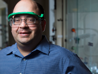
Dr. Claire M. Cobley, Managing Editor for ChemNanoMat, talks to Editorial Board Member Professor Javier Vela, Iowa State University, Ames, USA, about his article on germanium-based semiconductor nanoparticles that was recently published in ChemNanoMat.
Please could you briefly explain the focus and findings of your article and why it is of current interest?
Many technologically relevant semiconductors contain toxic and highly regulated elements such as cadmium, lead, or arsenic. Our new article in ChemNanoMat reports an aqueous synthesis of a lead-free alternative for lead-based halide perovskites. Germanium halide perovskite nanocrystals are a relatively new family of semiconductors that add to the growing number of alternative materials for photovoltaic solar cells and other energy conversion devices.
So to develop potentially more benign and less toxic lead-free alternatives, such as germanium halide perovskite nanocrystals, was your motivation behind this study?
Yes. And in addition to mitigating toxicity issues and the environmental footprint of halide perovskites, we are inorganic chemists who are constantly motivated by periodic properties. Moving ‘up and down’ a group, in this case replacing the central element in halide perovskites from Pb, to Sn, to Ge, and seeing what effect(s) this may have in the preparation and properties of materials, is always exciting to us.
You have explored the effects of manganese doping of perovskite nanocrystals. Why?
By doping magnetic ions into optically active materials, scientists hope to be able to use light to store and manipulate data at the single atom or quantum level. If a nanocrystalline host lattice is a sufficiently strong field, each one of the dopant Mn(II) ions will adopt a ‘high spin’ configuration with a maximum of five unpaired d electrons. Semiconductor nanocrystals are excellent hosts for these tiny magnets, provided their band gap—the minimum energy required for photoexcitation—is close in energy to the Mn(II) d electrons.
Lead-free perovskites seem to be a popular theme at the moment.
Yes, they are!
But what is it about your research that is particularly significant?
In the past we have also worked on lead-based halide perovskite nanocrystals, quite a bit. Actually, we systematically synthesize CH3NH3PbX3 (X = I, Br) nanocrystals with different morphologies such as dots, rods, plates or sheets by using different solvents and capping ligands. And then see how this correlates with photoluminescence. What is different about this new work in ChemNanoMat is that it is one of the very first papers to combine germanium and manganese in lead-free halide perovskite nanocrystals.
How will you follow up on this discovery?
Now that we know how to prepare and dope germanium halide perovskite nanocrystals, we really want to explore their use in photovoltaics. We want to use these materials to build working solar devices, and explore clever and simple ways that allow us to improve their long-term performance and stability.
How long do you think it will be before perovskite nanocrystals are used in real-life applications?
Not long! Thin film perovskite solar cells reached a certified power conversion efficiency (PCE) of 23.7 %, while nanocrystalline perovskite-based (quantum dot) solar cells reached a record PCE of 15.07 %. Further, these materials are cheap and easy to make. Therefore, there exist multiple powerful incentives for the deployment of these materials.
How long did your investigation take?
Quite a while! We started working on this project back in 2015. There were many hurdles and many new things to learn along the way, including updating reference data for ionic radii in order to more accurately interpret X-ray diffraction (XRD) data, as well as the better understanding the electron paramagnetic resonance (EPR) spectra of high-spin Mn(II) ions with six-coordinate halide coordination.
Why did you choose these techniques?
We specialize in colloidal semiconductors made by soft chemistry routes—usually mild temperatures, often in solution-phase. Both powder XRD and EPR techniques are commonly used in the characterization of doped semiconductors.
Which part of your work proved the most challenging?
As with lead-based halide perovskites, more work is needed to improve the shelf-stability of these materials. Of particular concern is their relative instability under conditions of excess moisture, heat, or under continuous illumination—nobody wants their solar cells to die when the sun is shining!
That’s true. What is the longer-term vision for your research?
We want to lead the design of distinct, powerful, and widely applicable synthetic strategies that span the continuum between molecular, nano, and bulk scales, and that enable the effective incorporation of new materials into innovative energy conversion and catalytic technologies.
The article they talked about
- Lead‐Free Semiconductors: Soft Chemistry, Dimensionality Control, and Manganese‐Doping of Germanium Halide Perovskites,
Long Men, Bryan A Rosales,Noreen E Gentry, Sarah D Cady, Javier Vela,
ChemNanoMat 2018.
https://doi.org/10.1002/cnma.201800497
The article is part of an upcoming special issue on Perovskite Nanocrystals.
[1] Feng Zhu, Long Men, Yijun Guo, Qiaochu Zhu, Ujjal Bhattacharjee, Peter M. Goodwin, Jacob W. Petrich, Emily A. Smith, Javier Vela, Shape Evolution and Single Particle Luminescence of Organometal Halide Perovskite Nanocrystals, ACS Nano 2015, 9(3), 2948–2959. https://doi.org/10.1021/nn507020s
[2] Michael P. Hanrahan, Long Men, Bryan A. Rosales, Javier Vela, Aaron J. Rossini, Sensitivity-Enhanced 207Pb Solid-State NMR Spectroscopy for the Rapid, Non-Destructive Characterization of Organolead Halide Perovskites, Chem. Mater. 2018, 30 (20), 7005–7015. https://doi.org/10.1021/acs.chemmater.8b01899


