Quantum Dots: Large Potential, Small Size
The term “quantum dot” (QD) was coined in 1988 by researchers at the well-known semiconductor company Texas Instruments, TI, Dallas, USA, to describe what is essentially a single-electron transistor, a nanoscopic semiconductor structure within which charged particles are confined in all three dimensions. The term encapsulated this concept of a three-dimensionally confined semiconductor quantum well, the kind of entity first identified in a glass matrix by solid-state physicist Alexei Ekimov at the beginning of the 1980s. The properties of QDs lie in that exotic middle ground between the bulk state of semiconductors, the familiar world of transistors and computer chips, and the behavior of individual molecules and atoms. As such, they hold great promise not only for bridging the potential gap between microelectronics and molecular electronics, but also through the manifestation of novel properties not observed in the bulk material or in single molecules.
Over the last three decades, countless researchers in materials, physics, chemistry, electronics, engineering, even biology and the multidisciplinary areas where the boundaries between fields are blurred, have turned to QDs as the new hope. QDs might even allow microelectronics to maintain Moore’s Law for decades to come. QDs might also lead to novel solar energy conversion and technology for quantum computing, as well as systems for biomedical research and medical diagnostics.
Underpinning the potential of QDs in a wide range of fields is the phenomenon that the dot’s electronic characteristics, the color with which it glows when stimulated, for instance, are tied closely to nothing more complicated than the size of the crystal. Scientists have found numerous ways to alter QDs’ size and so fine tune their properties. Larger dots are lower energy, lower frequency, which means they are redder, while smaller QDs shift towards the blue end of the spectrum.
Coupling Magnetic and Optical Properties
There is always room for further innovation in any field and ChemistryViews recently alerted readers to an important development in QDs stemming from an association between physicist Robert Meulenberg, University of Maine, USA, and chemist Geoffrey Strouse, Florida State University (FSU), Tallahassee, USA. The research carried out by Weiwei Zheng in the Strouse group in collaboration with colleagues at FSU, the Banaras Hindu University, Varanasi, India, the University of Maine, and the US National High Magnetic Field Laboratory, also in Tallahassee, Florida, has for the first time resulted in a magnetic spinel inclusion trapped within a QD crystal of chromium-doped zinc selenide.
“The research into spinel inclusions in a QD is the first reported example of an intentional inclusion with potential for magnetic applications,” Strouse told ChemViews magazine. “The idea stemmed from a published result on nano-inclusions in bulk materials for thermoelectrics,” he adds. “We pondered whether the same approach could be realized in a QD by controlling the reaction approach.”
The research points the way forward to extending the range of tunable properties of QDs and so to couple magnetic behavior to the size-dependent optical properties of the semiconductor QD in a field termed Dilute Magnetic Semiconductor Quantum Dots. The idea of a so-called DMSQD has been investigated theoretically and experimentally, but the ability to integrate a chromium(III)-based spinel into the semiconductor host could open up the possibility of using DMSQDs more explicitly for changing how electronic switching is controlled in circuits by coupling a magnet to the spin of electrons in the circuit, in the burgeoning field of “spintronics”. These materials could revolutionize the approach to quantum computing, magneto-resistive materials, photovoltaics, and magneto-optical applications, Strouse says.
Moreover, the research also highlights how a cross-disciplinary approach can push developments forward, given that some specialists tend to focus on the novel properties that might be induced in such a system, while others bring the skills to control the internal structure and chemistry and allow novel properties not only to emerge, but to be controlled.
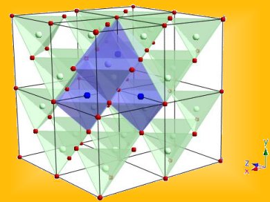
The team explain their achievement so far: “We report to the best of our knowledge the first study on Cr(III) incorporation into ZnSe QDs. The incorporation of chromium into a 2.8 nm ZnSe QD occurs as Cr(III) ions occupying a tetragonal distorted octahedral site within the cubic zinc selenide lattice, as evidenced by X-ray absorption near edge spectroscopy (XANES) and optical absorption crystal field analysis,” they say.
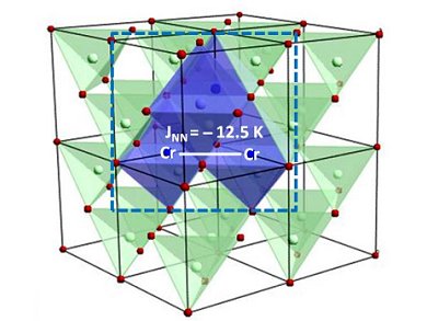
Figure 1. The structural inclusion of the Cr(III) center is believed to form ZnCr2Se4 unit cells precipitated within the ZnSe QD. Further evidence comes from the magnetic experimental data which includes an exchange coupling constant (JNN) of −12.5 K. ©: Geoffrey Strouse/Florida State University
“There is quite a bit more to do,” Strouse confessed to ChemViews magazine, “however, the approach opens a new frontier in QDs—namely use of intentional defects to manipulate the physical properties of materials at the nanoscale.” He adds that, “When we saw the XANES data we were quite excited. Such materials have real potential for development of spin valves and spin gates, in effect, alternative approaches to building electronics using a magnetic field to switch the electron flow. In addition, magneto-optical materials that display Faraday rotation or the Kerr effect, as well as thermoelectrics, and energy conversion materials in photovoltaics could be realized.”
Possible Applications of Dilute Magnetic Semiconductors
There are numerous teams targeting these so-called dilute magnetic semiconductors and hoping to incorporate magnetic ions or magnetic clusters within the lattice, including those of Pavle Radovanovic of the University of Waterloo, Ontario, Canada, Taeghwan Hyeon at Seoul National University, Jiye Fang at SUNY-Binghamton, New York, USA, Marie-Paule Pileni of the Université Pierre et Marie Curie and Centre National de la Recherche Scientifique, Paris, France, and Victor Klimov at Los Alamos National Laboratory, USA.
Daniel Gamelin at the University of Washington, USA, has led an effort in incorporating cobalt(II) and manganese(II) into metal oxides and chalcogenides. He told ChemViews magazine that the Strouse’s work is “exciting and unanticipated”. He adds that, “Further work may yield new forms of matter that possess unusual and exciting combinations of physical properties, such as magnetic order, semiconductivity, and luminescence, all on the nanoscale. The introduction of such unprecedented materials could impact the development of various technologies in exciting and unforeseen ways.”
Gamelin suggests that one particularly exciting aspect of the findings is that they evoke images of spinel-like clusters actually seeding II-VI QDs, rather than segregating from a uniform crystal via spinodal decomposition as in the analogous bulk materials. “As such, these findings suggest a rich variety of future experiments with potentially transformational outcomes,” he adds. “The main concept of the paper represents a terrific insight from the Strouse group that opens new directions in semiconductor research and development,” Gamelin concludes.
- Evidence of a ZnCr2Se4 Spinel Inclusion at the Core of a Cr-Doped ZnSe Quantum Dot,
W. Zheng, K. Singh, Z. Wang, J. T. Wright, J. van Tol, N. S. Dalal, R. W. Meulenberg, G. F. Strouse,
J. Am. Chem. Soc. 2012.
DOI: 10.1021/ja210285p - News: New Class of Quantum Dot,
D. Bradley,
ChemistryViews 2012.
First inclusion of Cr(III) spinel at the core of a quantum dot points the way to fine tuning the properties of QDs