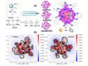
Jie Yao, University of California Berkeley, CA, USA, and colleagues have for the first time grown a crystal in spiral form from ultra-thin 2D layers. Initially, the team cultivated nanowires of germanium sulfide (GeS) by vapor deposition onto a substrate using a gold catalyst. When further evaporation took place, these nanowires grew to crystal towers up to 10 µm thick and several hundred micrometers long. These crystal towers are spirally wound. For inorganic materials, this is a rather exotic configuration.
Tiny defects with chiral symmetry in the crystal structure are the cause of this spiral rotation. The defects change the energy distribution, making the spiral form more energy-efficient. The phenomenon is called “Eshelby Twist”. According to the researchers, the angle between the layers could give the spiral crystals special optical, thermal, and electronic properties. The angle can be changed by adjusting the synthesis conditions and the length of the material.
So far, the researchers have only produced these spiral crystals from GeS and germanium selenide (GeSe). However, they suspect that such spiral crystal structures can also be produced from other materials with a layered basic structure.
- Helical van der Waals crystals with discretized Eshelby twist,
Yin Liu, Jie Wang, Sujung Kim, Haoye Sun, Fuyi Yang, Zixuan Fang, Nobumichi Tamura, Ruopeng Zhang, Xiaohui Song, Jianguo Wen, Bo Z. Xu, Michael Wang, Shuren Lin, Qin Yu, Kyle B. Tom, Yang Deng, John Turner, Emory Chan, Dafei Jin, Robert O. Ritchie, Andrew M. Minor, Daryl C. Chrzan, Mary C. Scott, Jie Yao,
Nature 2019, 570, 358–362.
https://doi.org/10.1038/s41586-019-1308-y