2D materials are an important class of nanomaterials. Transition metal dichalcogenides (TMDCs) represent the largest number of 2D materials. However, not all of these materials have been studied in-depth, and more work is needed to fully understand their different structures and properties.
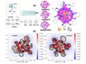
Jamie H. Warner and colleagues, University of Oxford, UK, have studied the atomic structure and dynamics of various defects and grain boundaries in 2D Pd2Se3 monolayers. The researchers first grew few-layered films of PdSe2 using chemical vapor deposition (CVD). Then they placed this compound in an annular dark field scanning transmission electron microscope (TEM). In the microscope, the films were heated and underwent an in-situ thermally-induced phase transformation, which promotes Se loss, converts the PdSe2 to a Pd2Se3 monolayer, and creates defects. Point vacancies, one-dimensional defects, grain boundaries, and defect ring complexes were also induced by irradiation with an electron beam.
The atomic vacancies were found to be highly mobile, which leads to the films self-healing under beam irradiation. They are stabilized by the formation of Se–Se bonds. Bond rotations were found to play a role in the defects and grain boundary dynamics: The grain boundaries migrate through a sequence of Se–Se bond rotations. At the corners of the grain boundaries, and in tilted grain boundaries, highly symmetric vacancies occur as a compensation mechanism for the orientation change. According to the researchers, this improved structural knowledge could help to find more possibilities for using these 2D materials through defect engineering.
- Atomic Structure and Dynamics of Defects and Grain Boundaries in 2D Pd2Se3 Monolayers,
Jun Chen, Gyeong Hee Ryu, Sapna Sinha, Jamie H. Warner,
ACS Nano 2019.
https://doi.org/10.1021/acsnano.9b03645