Graphene possesses outstanding electrical and thermal characteristics and has many possible applications. However, one stumbling block is that many unique properties and capabilities apply only to near-perfect graphene with a controlled number of defects. Defect-free graphene is difficult to prepare, and scanning large areas of graphene sheets in order to find defect locations and to estimate the quality of the material is time-consuming.
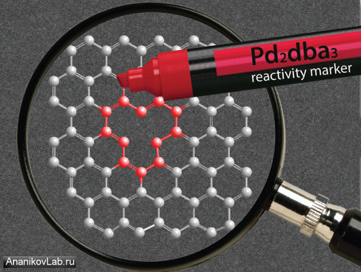
To locate graphene defects more easily, Valentine Ananikov, Zelinsky Institute of Organic Chemistry, Russian Academy of Sciences, Moscow, and colleagues have used the soluble palladium complex Pd2dba3 (dba: dibenzylideneacetone), which selectively attaches to defect areas on the surface of carbon materials. Attachment of the complex leads to the formation of Pd nanoparticles, which can be easily detected using electron microscopy.
More than 2000 reactive centers could be located per 1 μm2 of carbon material surface area. Thus, reactivity centers and defect sites on a carbon surface can be mapped in three dimensions with high resolution and excellent contrast.
- Spatial imaging of carbon reactivity centers in Pd/C catalytic systems,
E. O. Pentsak, A. S. Kashin, M. V. Polynski, K. O. Kvashnina, P. Glatzel, V. P. Ananikov,
Chem. Sci. 2015.
DOI: 10.1039/c5sc00802f