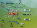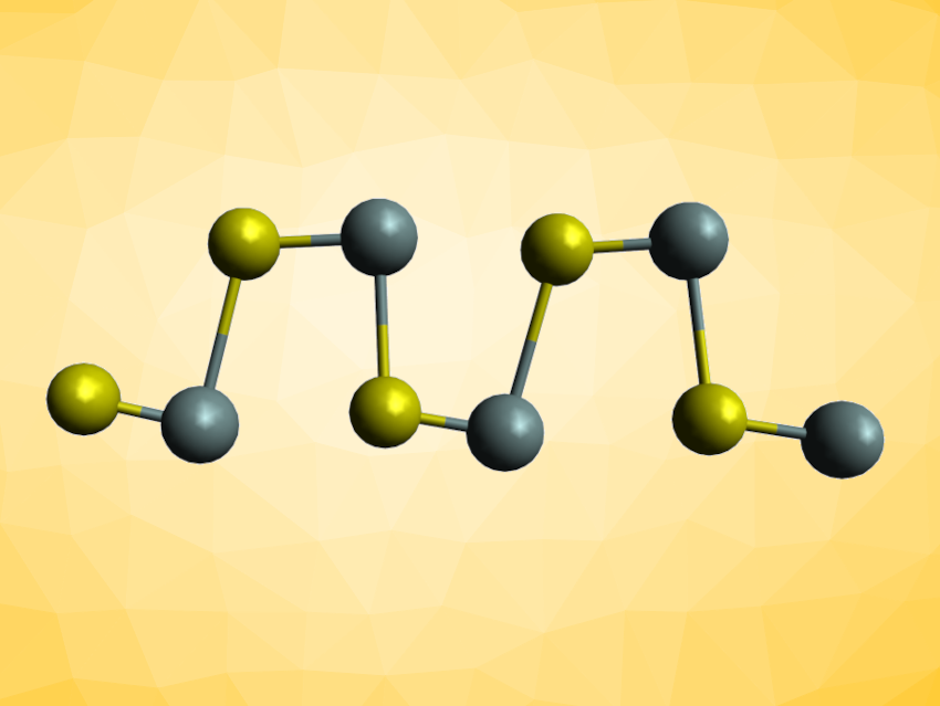
Two-dimensional materials consisting of atomically thin sheets can have useful properties. Reducing the materials to one-dimensional nanoribbons can be used to tune or enhance these properties and enable further applications. Layered monochalcogenides such as SnS, SnSe, GeS, or GeSe can be interesting as 2D materials. SnS, for example, is a semiconductor, and two-dimensional SnS has useful electronic and optoelectronic properties. However, its shape-controlled synthesis can be challenging.
Ye Wu, Wuhan University of Technology, China, Gonglan Ye, Hunan University, Changsha, China, and colleagues have developed an approach for the synthesis of highly crystalline SnS nanoribbons using high pressures (0.5 GPa) and temperatures (400 °C). The team first grew SnS2 flakes on a Si/SiO2 substrate using chemical vapor deposition (CVD) and then deposited the flakes on a sapphire substrate using a wet-transfer process. Then the reaction was performed under hydraulic pressure. At a pressure of 0.5 GPa and a temperature of 400 °C, a high density of SnS nanoribbons was obtained, distributed uniformly on the substrate.
Scanning electron microscopy (SEM) and atomic force microscopy (AFM) showed that the synthesized nanoribbons have lengths of several tens of micrometers and thicknesses of down to 5.8 nm. This corresponds to five SnS bilayers. The nanoribbons have a uniform crystal orientation along the “zigzag direction” of the structure. The team used the SnS nanoribbons in a field-effect transistor (FET) to investigate their electrical properties. The work could provide useful insights for the synthesis of 2D materials that are difficult to obtain at ambient pressure.
- High-Pressure Synthesis of Single-Crystalline SnS Nanoribbons,
Xinyu Zhang, Yuyang Shi, Zude Shi, Hang Xia, Mingyu Ma, Yiliu Wang, Kang Huang, Ye Wu, Yongji Gong, Huilong Fei, Yongmin He, Gonglan Ye,
Nano Lett. 2023.
https://doi.org/10.1021/acs.nanolett.3c01879
![]()