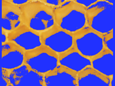
It has only been possible to see the crystal structure of a material by looking at a cut surface, giving 2D information. In recent years, x-ray methods have been developed that can be used to look inside a material and obtain a 3D map of the crystal structure. These methods have a resolution limit of around 100 nm.
Scientists from Risø DTU, Denmark, in collaboration with scientists from Tsinghua University, China, Shenyang National Laboratory for Materials Science, IMR, China, and Johns Hopkins University, USA report a newly developed technique allowing 3D mapping of the crystal structure inside a material down to nanometer resolution. It has a resolution 100 times better than existing non-destructive 3D techniques. It can be carried out using a transmission electron microscope.
It opens up new opportunities for more precise analysis of the structural parameters in nanomaterials and allows the changes taking place inside a material to be observed directly. For example, the mapping may be repeated before and after a heat treatment revealing how the structure changes during heating.
- Three-Dimensional Orientation Mapping in the Transmission Electron,
H. H. Liu et al.
Science 2011, 332 (833).
DOI: 10.1126/science.1202202