Photocatalytic activity, electrical conductivity, and optical properties of p–type semiconducting Cu2O nanocrystals show a strong direction dependence. Various crystal facets have different band structures and conductivities.
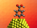
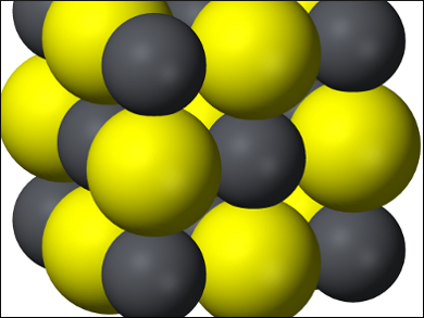
Michael Huang, National Tsing Hua University, Hsinchu, Taiwan, and colleagues wondered whether the n–type semiconductor PbS would exhibit the same variations. They grew PbS nanocrystals with sizes of at least 200 nm and with facets oriented along various crystallographic planes. They showed that, in positively and negatively charged solutions, the PbS {110} and {100} faces are highly conductive at applied voltages larger than 4 V, but the {111} faces remain nonconductive even at 5 V. Density of state calculations for various PbS layers and planes showed differences in the areas of the conduction bands as far as 3.0–3.4 nm beneath the surface.
These results correlate well with the observed electrical conductivity, and they give an approximation of the thickness of the surface layers responsible for the facet dependence. The insight might be useful in constructing nanoscale electronic components.
- Facet-Dependent Electrical Conductivity Properties of PbS Nanocrystals,
Chih-Shan Tan, Hsiang-Sheng Chen, Chun-Ya Chiu, Szu-Chieh Wu, Lih-Juann Chen, Michael H. Huang,
Chem. Materi. 2016.
DOI: 10.1021/acs.chemmater.6b00274