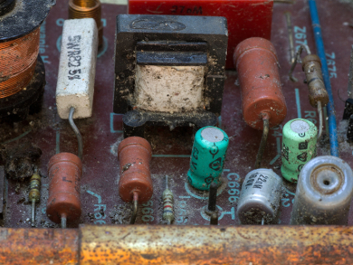
Increased production, demand, and use of electronic equipment, such as wrist watches, computers and mobile phones, is leading to massive waste generation. E-wastes consist of semiconductor materials, including n-type and p-type materials. N-type consist of Bi2Te3 and p-type consist of Sb2Te3 or Bi0.5Sb1.5Te3. These semiconducting materials have been shown to be poisonous, causing diminished learning abilities of children, reduced fertility through sperm damage, subtle abortions, disruption of the nervous system, eye irritation, depression and stomach problems.
Basuden Swain, Advanced Materials & Processing Center, and Kun-Jae Lee, Dankook University, Republic of Korea, have developed a new technique for treatment, remediation, and reuse of hazardous soldering materials mainly consisted of Pb and Sn. They successfully separated p- and n-type chips through HNO3 dissolution by thermal treatment followed by chemical dissolution. The separated p-type can be reused in thermoelectric modules. From the n-type, a Bi2Te3 nanopowder was synthesized through wet chemical reduction using hydrazine for reuse in n-type chips manufacturing.
The developed e-waste management process is clean, green and techno-economically feasible for the treatment and remediation of hazardous soldering material. It also adds value through the recovery of industrially important metals such as bismuth, tellurium, and antimony.
- Chemical separation of p- and n-type thermoelectric chips from waste thermoelectric module and valorization through synthesis of Bi2Te3 nanopowder: a sustainable process for synthesis of thermoelectric materials,
Basudev Swain, Kun-Jae Lee,
J. Chem. Technol. Biotechnol. 2016.
DOI: 10.1002/jctb.5042